FPGA Prototyping by VHDL Examples
 -15%
portes grátis
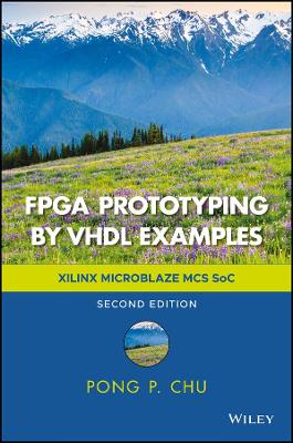
FPGA Prototyping by VHDL Examples
Xilinx MicroBlaze MCS SoC
Chu, Pong P.
John Wiley & Sons Inc
12/2017
632
Dura
Inglês
9781119282747
15 a 20 dias
1258
Acknowledgments xv
PART I BASIC DIGITAL CIRCUITS DEVELOPMENT
1 Gate-level Combinational Circuit 1
1.1 Overview of VHDL 1
1.2 General description 2
1.3 Structural description 6
1.4 Top-level signal mapping 8
1.5 Testbench 9
1.6 Bibliographic notes 11
1.7 Suggested experiments 11
2 Overview of FPGA and EDA software 13
2.1 FPGA 13
2.2 Overview of the Digilent Nexys 4 DDR board 15
2.3 Development flow 16
2.4 Xilinx Vivado Design Suite 18
2.5 Bibliographic notes 18
2.6 Suggested experiments 18
3 RT-level combinational circuit 23
3.1 RT-level components 23
3.2 Routing circuit with concurrent assignment statements 29
3.3 Modeling with a process 34
3.4 Routing circuit with if and case statements 36
3.5 Constants and generics 41
3.6 Replicated structure 44
3.7 Design examples 46
3.8 Bibliographic notes 58
3.9 Suggested experiments 58
4 Regular Sequential Circuit 61
4.1 Introduction 61
4.2 HDL code of the FF and register 64
4.3 Simple design examples 67
4.4 Testbench for sequential circuits 72
4.5 Case study 75
4.6 Timing and clocking 87
4.7 Bibliographic notes 90
4.8 Suggested experiments 90
5 FSM 93
5.1 Introduction 93
5.2 FSM code development 97
5.3 Design examples 100
5.4 Bibliographic notes 110
5.5 Suggested experiments 110
6 FSMD 113
6.1 Introduction 113
6.2 Code development of an FSMD 119
6.3 Design examples 125
6.4 Bibliographic notes 140
6.5 Suggested experiments 141
7 RAM and Bu?er of FPGA 145
7.1 Embedded memory of FPGA device 145
7.2 General description for RAM-like component 147
7.3 FIFO bu?er 153
7.4 HDL templates for memory inference 158
7.5 Overview of memory controller 164
7.6 Bibliographic notes 166
7.7 Suggested experiments 166
PART II EMBEDDED SOC I: VANILLA FPRO SYSTEM
8 Overview of Embedded SoC Systems 171
8.1 Embedded SoC 171
8.2 Development Flow of Embedded SoC 173
8.3 FPro SoC Platform 176
8.4 Adaption on Digilent Nexys 4 DDR board 180
8.5 Portability 182
8.6 Organization 184
8.7 Bibliographic notes 184
9 Bare Metal System Software Development 187
9.1 Bare metal system development overview 187
9.2 Memory-mapped I/O 189
9.3 Direct I/O Register Access 191
9.4 Robust I/O Register Access 193
9.5 Techniques for low-level I/O operations 197
9.6 Device Drivers 199
9.7 FPro Utility Routines and Directory Structure 204
9.8 Test program 208
9.9 Bibliographic notes 211
9.10 Suggested experiments 211
10 FPro Bus Protocol and MMIO Slot Specification 213
10.1 FPro Bus 213
10.2 Interface with bus 216
10.3 MMIO I/O core 222
10.4 Timer core development 226
10.5 MMIO controller 229
10.6 MCS I/O bus and bridge 234
10.7 Vanilla FPRO System Construction 238
10.8 Bibliographic notes 240
10.9 Suggested experiments 240
11 UART Core 243
11.1 Introduction 243
11.2 UART Construction 245
11.3 UART core development 253
11.4 UART driver 256
11.5 Additional Project Ideas 262
11.6 Bibliographic notes 265
11.7 Suggested experiments 266
PART III EMBEDDED SOC II: BASIC I/O CORES
12 Xilinx XADC Core 271
12.1 Overview of XADC 271
12.2 XADC core development 273
12.3 XADC core device driver 278
12.4 Sampler FPro System 281
12.5 Additional Project Ideas 291
12.6 Bibliographic notes 292
12.7 Suggested experiments 292
13 Pulse Width Modulation Core 295
13.1 Introduction 295
13.2 PWM Design 296
13.3 PWM core development 299
13.4 PWM driver 302
13.5 Testing 303
13.6 Project ideas 304
13.7 Suggested experiments 305
14 Debouncing core and LED-Mux Core 307
14.1 Debouncing Core 307
14.2 LED-Mux Core 313
14.3 Project Ideas 319
14.4 Suggested Experiments 320
15 SPI Core 323
15.1 Overview 323
15.3 SPI Core Development 333
15.4 SPI Driver 336
15.5 Test 338
15.6 Project Ideas 341
15.7 Bibliographic notes 342
15.8 Suggested Experiments 342
16 I2C Core 347
16.1 Overview 347
16.2 I2C Controller 350
16.3 I2C Core Development 360
16.4 I2C Driver 361
16.5 Test 365
16.6 Project Idea 366
16.7 Bibliographic notes 367
16.8 Suggested experiments 367
17 PS2 Core 371
17.1 Introduction 371
17.2 PS2 Controller 373
17.3 PS2 core development 383
17.4 PS2 driver 384
17.5 Test 393
17.6 Bibliographic notes 394
17.7 Suggested experiments 394
18 Sound I: DDFS Core 397
18.1 Introduction 397
18.2 Design and implementation 397
18.3 Fixed-point arithmetic 400
18.4 DDFS Construction 402
18.5 DAC (digital-to-analog converter) 404
18.6 DDFS core development 407
18.7 DDFS driver 409
18.8 Testing 412
18.9 Bibliographic notes 413
18.10 Suggested experiments 413
19 Sound II: ADSR Core 415
19.1 Introduction 415
19.2 ADSR envelope generator 416
19.3 ADSR core development 421
19.4 ADRS driver 423
19.5 Testing 429
19.6 Project Idea 430
19.7 Bibliographic notes 431
19.8 Suggested experiments 431
PART IV EMBEDDED SOC III: VIDEO CORES
20 Introduction to Video System 435
20.1 Introduction to a video display 435
20.2 Stream interface 437
20.3 VGA Synchronization 439
20.4 Bar test-pattern generator 448
20.5 Color-to-grayscale conversion circuit 449
20.6 Demo video system 451
20.7 Advanced video standards 452
20.8 Bibliographic notes 453
20.9 Suggested experiments 454
21 FPro Video Subsystem 457
21.1 Organization of video subsystem 457
21.2 FPro video IP core 461
21.3 Example video cores 466
21.4 FPro video synchronization core 470
21.5 Daisy video subsystem 479
21.6 Vanilla daisy FPro system 486
21.7 Video driver and testing program 490
21.8 Bibliographic notes 493
21.9 Suggested experiments 493
22 Sprite Core 497
22.1 Introduction 497
22.2 Basic design 498
22.3 Mouse pointer core 500
22.4 "Ghost" character core 505
22.5 Sprite core driver and testing program 513
22.6 Bibliographic notes 516
22.7 Suggested experiments 516
23 On-Screen-Display Core 519
23.1 Introduction to tile graphics 519
23.2 Basic OSD design 521
23.3 OSD core 524
23.4 OSD core driver and testing program 530
23.5 Bibliographic notes 532
23.6 Suggested experiments 532
24 VGA Frame Bu?er Core 535
24.1 Overview 535
24.2 Frame bu?er core 536
24.3 Register map 540
24.4 Driver and testing program 542 543
24.5 Project Ideas 545
24.6 Bibliographic notes 547
24.7 Suggested experiments 547
PART V EPILOGUE
25 What Next 553
References 557
Appendix A: Tutorials 561
A.1 Overview of Xilinx Vivado IDE 561
A.2 Short tutorial on Vivado hardware development 565
A.3 Short tutorial on Vivado simulation 570
A.4 Tutorial on IP instantiation 574
A.5 Short tutorial on FPro system development 580
A.6 Bibliographic notes 587
Topic Index 589

